Programmer and debugger ports
Debugging
Adding a debugger port allows programmers to set breakpoints, step through the running code and flash new bootloader and firmware binaries onto the device.
There are two debug protocols: JTAG and SWD. JTAG uses 20 pins, and is able to power the MCU directly from the debugger. Additionally, it allows access to more signals provided by the MCU. SWD uses 4 to 6 pins and only supports the slightly more limited SWD protocol.
For simplicity, only the SWD interface is explained here.
6 vs 10 vs 20 pin connectors
The number of connectors is a tradeoff between connector size and feature richness of the debugger. Generally, the following (dis-)advantages exist:
- 6 pin: SWD only, very little space required, no connector required.
- 10 pin: SWD and JTAG, little space required, no connector required, able to power target.
- 20 pin: ???
SWD interface
ARM processors usually use the SWD (Serial Wire Debug) interface. It consists of the following pins:
| Pin | Type | Description |
|---|---|---|
| VREF | Output | Target voltage |
| SWDIO | Bidirectional | Data pin |
| SWCLK | Output | Clock signal |
| GND | - | Ground level |
| SWO | Output | Optional: trace output |
Debug probes
Many debug probes are available. The following information is for the Black Magic Probe.
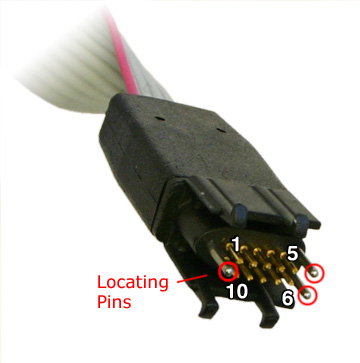
The connector pins are laid out as follows (the names in brackets are the configuration of the nrf9160 DK). Only VTREF, SWDIO, SWCLK and GND are required. The signals TMS/TCK/TDO/TDI are from the JTAG standard and are not required for SWD debugging.
| Notch | Column 1 | Column 2 |
|---|---|---|
| 1 VTREF | 2 SWDIO/TMS | |
| 3 GND | 4 SWCLK/TCK | |
| [ | 5 GND | 6 SWO/TDO |
| 7 NC | 8 TDI/(NC) | |
| 9 NC/(GND) | 10 nRESET |
There is a 6 pin version available with the following pin functions (⦻ is for the alignment hole). A 10-pin-to-6-pin adapter is required.
| Column 1 | Column 2 |
|---|---|
| ⦻ | |
| 1 VTREF | 2 SWDIO |
| 3 nRESET | 4 SWCLK |
| 5 GND | 6 SWO |
| ⦻ | ⦻ |
Debug connectors
The debugger can be connected to the target in multiple ways:
- Placing a header with pins on the board: easy to solder, uses much space.
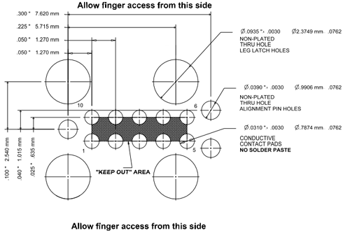
- Exposing the copper of the SWD traces on the board, along with alignment and latch holes, to be used with a needle adapter: no soldering, easy to attach the adapter.
- Exposing the copper of the SWD traces with alignment holes for a needle adapter without leg latches: no soldering, adapter must be pushed down on the board manually.
The options are explained below.
Header
Use a 2x5 pin header with 1.27mm connector spacing on the board. You can optionally use a one-way shroud to ensure the connector is plugged in the right way.
Needle adapter with latches
The nrf9160 DK uses exposed pads compatible with the “TC2050-IDC” connector.


Needle adapter without latches
The option without latches does not require the latch holes of the above drawing. This makes the footprint a lot smaller, but might not be equally convenient.
This option is compatible with the “TC2030-IDC-NL” connector.